SerDes clocking catered to robust noise handling in advanced process technologies for HPC, Datacenter, 5G and AI applications
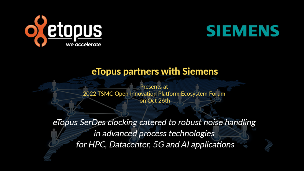
Find out how eTopus aids high-speed data center links needed to support a wide span of data rates and protocols, employing complex modulation schemes and varying insertion loss requirements from VSR at few dBs to LR at 35+ dB
October 26, 2022
 Abstract
The technological world continues to witness tremendous growth in information traffic, fueled by the digital transformation of businesses over the last 5 years. The wide adoption of cloud has driven substantial demand for data bandwidth. The number of hyperscale data centers has doubled since and is currently more than five hundred. This trend continues to gain momentum. The end-to-end Information traffic from enterprise data center to cloud data center, to Edge, to 5G infrastructure requires SerDes interfacing that provide the communication gateway into, within, between and outside chips. These high-speed links need to support a wide span of data rates and protocols employing complex modulation schemes and varying insertion loss requirements from Very Short Reach (VSR) at few dBs to Long Reach (LR) at 35+ dB. Furthermore, the requirement to traverse the network with backplane, cable, or optical media reaches from a few inches to tens of kilometers, or from within data center to outdoor in harsh environment. The diverse applications and requirements of SerDes in turn poses design challenges for accurate data and clock recovery with stringent jitter requirements requiring innovative equalization architectures to compensate for channel loss and cross talk.
eTopus Technologies is a US based start-up with design centers also in Hong Kong and Taiwan developing ultra-high speed mixed-signal semiconductor solutions for HPC, data center, networking, storage, 5G and AI applications. TSMC has been our foundational partner in providing reliable and scalable cutting-edge process technologies with ease of integration from 0.5um through 5nm. They enable us to achieve high complexity, high performance and low power designs and applications to meet our customer requirements. eTopus has demonstrated multiple generations of ADC/DSP-based PAM-4 SerDes IP to support multiple data rates such as PCIe Gen6, 56Gbps and 112Gps using TSMC 28nm, 22nm, 16nm, 12nm, and 7nm with superior BER performance, and we continue to develop future generation designs with advanced TSMC technology.
eTopus uses Siemens EDA’s Analog FastSPICE Platform (AFS) for circuit verification and sign-off. To meet or exceed quality requirements with faster time to market, an accurate, fast and versatile simulator is required to handle various netlist constructs (schematic and extracted including S-Parameters, leaf and upper levels) for functional, test and reliability analyses. With AFS, designers can architect, experiment, and finalize analog circuits of varying sizes with DC, transient and RF analyses including noise for creating robust SerDes IPs with increased productivity and time to market, with augmented support of other Siemens EDA front and back end verification software.
In this paper, we delve into clock distribution, a critical make or break entity, for high speed SerDes designs that demand stringent jitter requirements. Fabricated in advanced TSMC FinFET 7nm process, we will showcase the design and verification of 13.28125GHz clock paths within transceivers utilizing RF Shooting Newton and Transient noise analyses bridging it to silicon correlation for jitter and signal integrity specifications for 106.25Gbps.
Reference: TSMC OIP – Session Information (pl-marketing.biz)

